
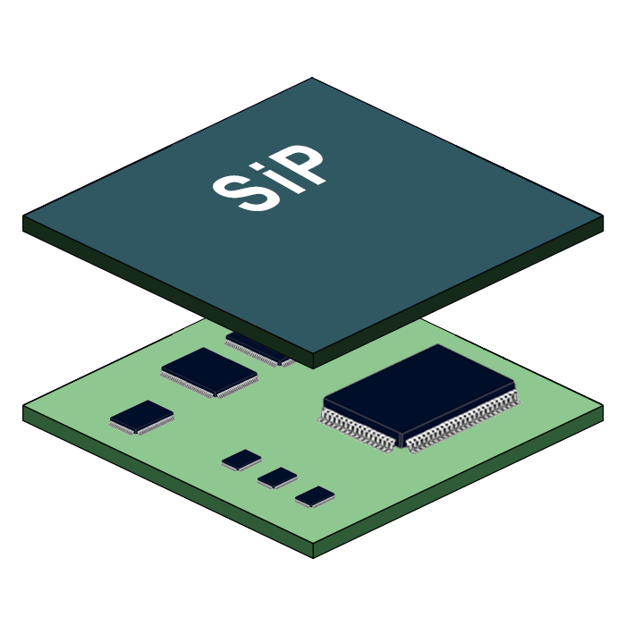
Research Semi
Integrated circuit (IC) chips are inspected at various stages during the design and testing phases, and highly accurate microscopes are critical to this process. Observing the Surface of IC Chips Integrated circuit (IC) design companies need to inspect the pattern of designed IC chips. Additionally, IC chip manufacturers must analyze the IC chip design at the trial production step. Since the inspection volume is low, manufacturers can use manual equipment with high accuracy. Our Solution Our BX/MX series industrial microscopes feature magnification as high as 1,000X, enabling you to observe IC patterns with lines in the micrometer or sub-micrometer level. Alternatively, our DSX series microscopes offer magnification as high as 7,000X and are easy to operate.

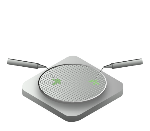
Slice the ingot into thin silicon plates (wafers). Polish the top and bottom of the wafer surfaces. This flattens the surface so the circuit patterns can be imprinted. The polished wafer is then marked with laser marking equipment.Inspecting the Surface Roughness of a Wafer The wafer’s surface must be properly flattened to imprint precise IC patterns on it. As a result, detailed inspections of the surface roughness are required after polishing. Our Solution Our OLS series microscopes can show the surface roughness conditions of a wafer in fine detail after the surface polishing step. It can also measure the surface roughness at both the micro and nano level.

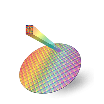
Photolithography is the process of imprinting integrated circuit patterns on the wafer. This process is repeated several times to make complex circuit patterns.Measuring the Resist Thickness in the Photoresist Process The inspector prints the designed pattern on the silicon wafer using photolithography. Managing the thickness of the resist is critical to correctly print the pattern on the wafer. Our Solution With QWP filters, our OLS5000 laser confocal microscope can remove the scattered light effect from the silicon and accurately capture the surface profile. Skip scan mode also helps with fast acquisition.
Check if the wafer runs correctly with an electronics tester called a prober.Measuring Probe Mark Dimensions During the electrical test of IC chips, the prober’s testing pin scratches the chips' aluminum pads. If the scratch mark is large, the electrical conductivity conditions on the aluminum pads will decay and affect the wire bonding process. As a result, the dimensions of the scratch marks must be measured.Our Solution Our DSX1000 digital microscope can capture 3D images and provide 3D measurements, enabling you to measure the scratch mark’s depth and width.
Print a product name on the IC package using laser marking. Inspecting the Appearance of Markings The legibility of laser markings is important since the automation system sorts and places IC chips as it identifies the markings. Yet, microscope observation of the marking on a black resin package is difficult due to glare caused by the microscope’s illumination. Our Solution Our DSX1000 digital microscope acquires clear images of laser markings without glare thanks to its high dynamic range (HDR) function.
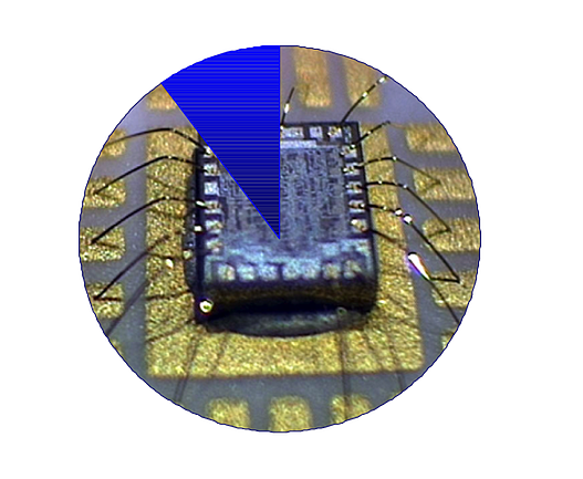
An IC chip connects to external devices with wire bonding. Wire bonding is a method to weld between an IC chip and the lead frames. A wire is attached to a lead frame and an IC chip's aluminum pad using a combination of downward pressure, ultrasonic energy, and heat to make a weld. Analyzing the Surface Conditions of Lead Frames An IC chip and the inner leads of lead frames are connected by bonding wires. Uneven surfaces on the leads can cause faulty adhesive wire bonding, so it is important to measure the leads’ surface roughness. Another challenge is that as IC packages downsize, the leads became thinner. Our Solution Our OLS series microscope can image ultra-fine leads for roughness measurement. Roughness of the lead frame is managed by an R ratio, and the OLS series has the necessary parameter.